
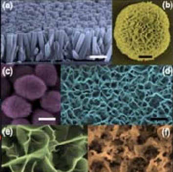
Experimental physics of matter
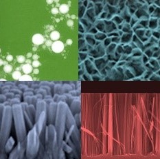
The group conducts experimental studies of phenomena related to the structure of materials and their mesoscopic properties, both on massive materials and on thin films and nanostructures. It comprisees 15 units including teachers and researchers, supported by 15-20 PhD students, undergraduates and postdocs, and has a very wide variety of synthesis, analysis and prototyping techniques on over 1000 m2 of laboratories at the DFA, partly in agreement with CNR-IMM. Many activities are carried out in collaboration with other Italian and foreign universities, and with large companies (STMicroelectronics, Enel Green Power, ...) in the local geographical area. The research activity ranges from the synthesis of innovative materials with nanometric dimensions to structural, electrical, optical and electrochemical characterization, up to the creation of simple prototype devices. The materials under study are metals, insulators and solid phase semiconductors, for which the morphological and structural, optical, electrical and electrochemical properties are correlated. The fields of application vary from microelectronics to photonics, from energy to sensors.
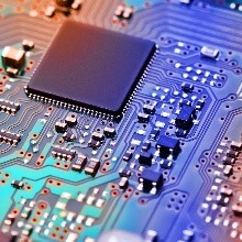
Microelectronics
Faculty: S. Boscarino, L. Calcagno, M.G. Grimaldi, G. Mineo, S. Mirabella, A. Scandurra, A. Terrasi, F. Torrisi
In the "post-silicon" era of microelectronics, numerous research efforts are aimed at developing innovative materials with superior performances. Wide bandgap semiconductors are largely studied for power devices, while thin films of transparent and conductive materials find application in both solar cells and touch screen devices. Ultra-thin materials (down to the thickness of a single atom) are being investigated to develop applications of printable, inexpensive and flexible electronics.
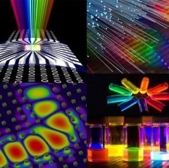
Photonics
Faculty: S. Boscarino, M.R. Chiechio, M. J. Lo Faro, P. Musumeci, F. Priolo, R. Reitano, F. Torrisi
Silicon-based photonics allows data transfer at speeds significantly higher than conventional electronics, while allowing integration with electronic devices on the market. The decades-long experience of the group in this field has made it possible to obtain important results in the field of optoelectronics, plasmonics and photonics, creating for Si-based devices for the emission of light through the nanostructuring of the material (nanocrystals or nanowires of silicon) and the use of rare earths (Er, Eu, Y or composite systems).
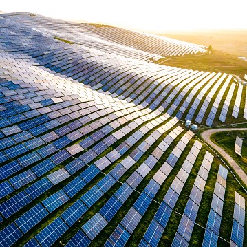
Energy
Faculty: S. Boscarino, E. Bruno, G. Mineo, S. Mirabella, F. Ruffino, M.C. Spadaro, A. Terrasi, M. Urso
The development of innovative materials for the energy scenarios of the future today plays a leading role in the green transition. Among the various challenges for sustainable progress there are certainly new materials that improve the performance of light-energy conversion, nanostructured materials that can catalyze water electrolysis and hybrid systems capable of accumulating large amounts of energy in very small volumes. In all these research fields, the physics of matter allows an investigation that is always original and winning for the in-depth understanding of the structural and electronic properties at play.
Sensors
Faculty: S. Boscarino, E. Bruno, M.R. Chiechio, M.G. Grimaldi, M. J. Lo Faro, S. Mirabella, P. Musumeci, F. Priolo, F. Ruffino, A. Scandurra, M.C. Spadaro, F. Torrisi, M. Urso
Sensors play an essential role in numerous sectors of interest for the Internet of Things, from home automation to automotive, biomedical engineering to the food and packaging sector or even precision agriculture. The physics of matter contributes to the understanding of microscopic phenomena underlying the detection mechanism and reveals the interactions that occur at the interface between the sensitive material and the surrounding environment. The long experience of the group in the physics of materials and the consolidated experience in controlling their morphology and their dimensions, has allowed to develop innovative nanostructures applied in simple demonstration devices with high performance.