
Photonics
.jpg)
Silicon-based photonics allows data transfer at speeds significantly higher than conventional electronics, while allowing integration with electronic devices on the market. The decades-long experience of the group in this field has made it possible to obtain important results in the field of optoelectronics, plasmonics and photonics, creating for Si-based devices for the emission of light through the nanostructuring of the material (nanocrystals or nanowires of silicon) and the use of rare earths (Er, Eu, Y or composite systems).
Photonics Materials
Faculty: M. J. Lo Faro, P. Musumeci, F. Priolo
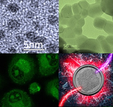
The control of interaction of matter radiation allows to improve the optical responses of a material and to increase the performance of optoelectronic devices. The synthesis of nanostructured materials of different compositions, dimensions and geometries makes it possible to exploit the engineering of materials for light management through the correlation of structural and optical parameters for applications from biotargeting, bioimaging and construction of optoelectronic devices. In addition, the development of polymer composites based on 2D materials for ultra-wideband applications in ultra-fast pulsed lasers and light diffusers is underway.
Plasmonics Materials
Faculty: S. Boscarino,M. J. Lo Faro,F. Ruffino
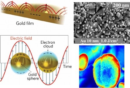
The metallic nanostructures of Au, Ag, Cu, Al present, in the interaction with electromagnetic radiation, plasmonic properties that make them optimal candidates for use in solar cells in view of increasing their efficiency. This activity foresees the controlled production in size and shape of nanostructures of Au, Ag, Cu, Al (exploiting approaches based on laser ablation, dewetting of deposited films) and their integration with transparent and conductive oxides and, finally, the elttro characterization - optics of the resulting composites.