
Quantum nanostructures at atomic scale
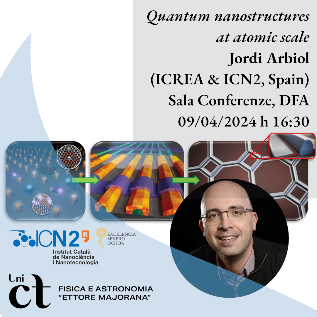
Giorno 9 aprile 2024, con inizio alle ore 16:30, presso la Sala Conferenze del DFA, il Prof. Jordi Arbiol (ICREA & ICN2, CSIC and BIST, Barcelona, Spain) terrà un seminario dal titolo Quantum nanostructures at atomic scale: From vertical hybrid nanowires to planar nanowire networks and 2DEG/2DHG systems.
Il seminario è organizzato dalla Prof.ssa Maria Chiara Spadaro e dal Prof. Salvo Mirabella.
Tutte le persone interessate sono invitate a partecipare.
Abstract. Hybrid superconductor/semiconductor-based quantum devices (e.g.: for quantum computing applications) are mainly based on 3 di erent technologies: vapour-liquid-solid (VLS) grown vertical nanowires, selected area growth (SAG) nanowire networks and 2-dimensional electron gases (2DEG). First of all, by using atomic-scale aberration corrected Scanning Transmission Electron Microscopy (AC STEM) and 3D modelling, we will study the influence of polarity on the development and properties of these complex NW-like hybrid heterostructures vertically grown by VLS [1-3].
In a second part, we will show the natural evolution of this vertical technology to the flat growth of NW networks on III-V substrates. Developing growth techniques towards horizontally assembled semiconductor nanowire networks base on SAG is essential to promote their integration into large-scale functional circuit platforms and devices for electronic, photonic and quantum applications and more over to address a high scalability. In these complex core@shell or confined multilayer nanostructure configurations, strain relaxation mechanisms during the epitaxial growth play a key role in determining their final morphology, crystal structure and physical properties. To analyze these mechanisms, in the present work, atomic-scale Cs-corrected Scanning Transmission Electron Microscopy studies are performed on horizontal arrays of nanowires. Core morphology-dependent strain fields, involving plane bending and the resulting formation of low angle polar boundaries, are observed. The origin of this phenomenon and its consequences on the electronic band structure are discussed. Monochromated Valence Electron Energy Loss Spectroscopy is employed to spatially map the heterostructure’s bandgap with sub-nanometer resolution and certify the influence of the high mismatch induced strain on the topological electronic properties at the interface of the core-shell region. These findings highlight the importance and potential of accurate sub-nanometer-level understanding of the structure-property relations in the novel SAG and guided growth mechanisms of heterostructured semiconductor nanowire networks [4-6].
Finally, we will address the newly developed 2DEG heterostructures based on SiGe, fully compatible with CMOS technology, were the strain and composition at the Ge quantum wells will determine their final quantum properties [7-8].
References.
- [1] M. de la Mata, et al., Nano Letters, 19, 3396 (2019)
- [2] M. Zamani, et al., Advanced Materials, 32, 2001030 (2020)Scientific Seminar
- [3] M. Valentini, et al., Nature, 612, 442 (2022)
- [4] E. Oksenberg, et al., ACS Nano, 11, 6155 (2017)
- [5] M. Friedl, et al., Nano Letters, 18, 2666 (2018)
- [6] S. Martí-Sánchez, M. Botifoll, et al., Nature Commun., 13, 4089 (2022)
- [7] D. Jirovec, et al., Nature Materials, 20, 1106 (2021)
- [8] B. Paquelet Wuetz, et al., Nature Commun., 14, 1385 (2023)
Bio. Graduated in Physics at Universitat de Barcelona (UB) in 1997, where he also obtained his PhD (European Doctorate and PhD Extraordinary Award) in 2001 in the field of transmission electron microscopy (TEM) applied to nanostructured materials. He also worked as Assistant Professor at UB. In 2009 he was appointed as ICREA Professor and holds this position since then. From 2009 to 2015 he was Group Leader at Institut de Ciència de Materials de Barcelona, ICMAB-CSIC and Scientific Supervisor of its electron microscopy facilities. He was the President of the Spanish Microscopy Society (SME) from 2017 to 2021, was Vice-President from 2013 to 2017 and from 2009 to 2021 he was Member of its Executive Board. In 2018 he was elected as Member of the Executive Board of the International Federation of Societies for Microscopy (IFSM) (2019-2026). Since 2015 he is the leader of the Group of Advanced Electron Nanoscopy at Institut Català de Nanociència i Nanotecnologia (ICN2), CSIC and BIST. He is Scientific Supervisor of the Electron Microscopy Area at ICN2 and BIST and the Scientific Coordinator of the Materials area at Joint Electron Microscopy Center at ALBA Synchrotron (JEMCA). He has been one of the founder members of e-DREAM. Since 2023 he is Associate Editor of Nano Letters (American Chemical Society). He received the FWO Commemorative Medal (Flanders Research Foundation) in 2021, the 2018 BIST IGNITE Award and was awarded with the EU40 Materials Prize 2014 (E-MRS), 2014 EMS Outstanding Paper Award and listed in the Top 40 under 40 Power List (2014) by The Analytical Scientist. In February 2024, he has co-authored more than 475 publications with 30.900+ citations and h-index: 98 (GoS).