Exploring matter at the atomic level

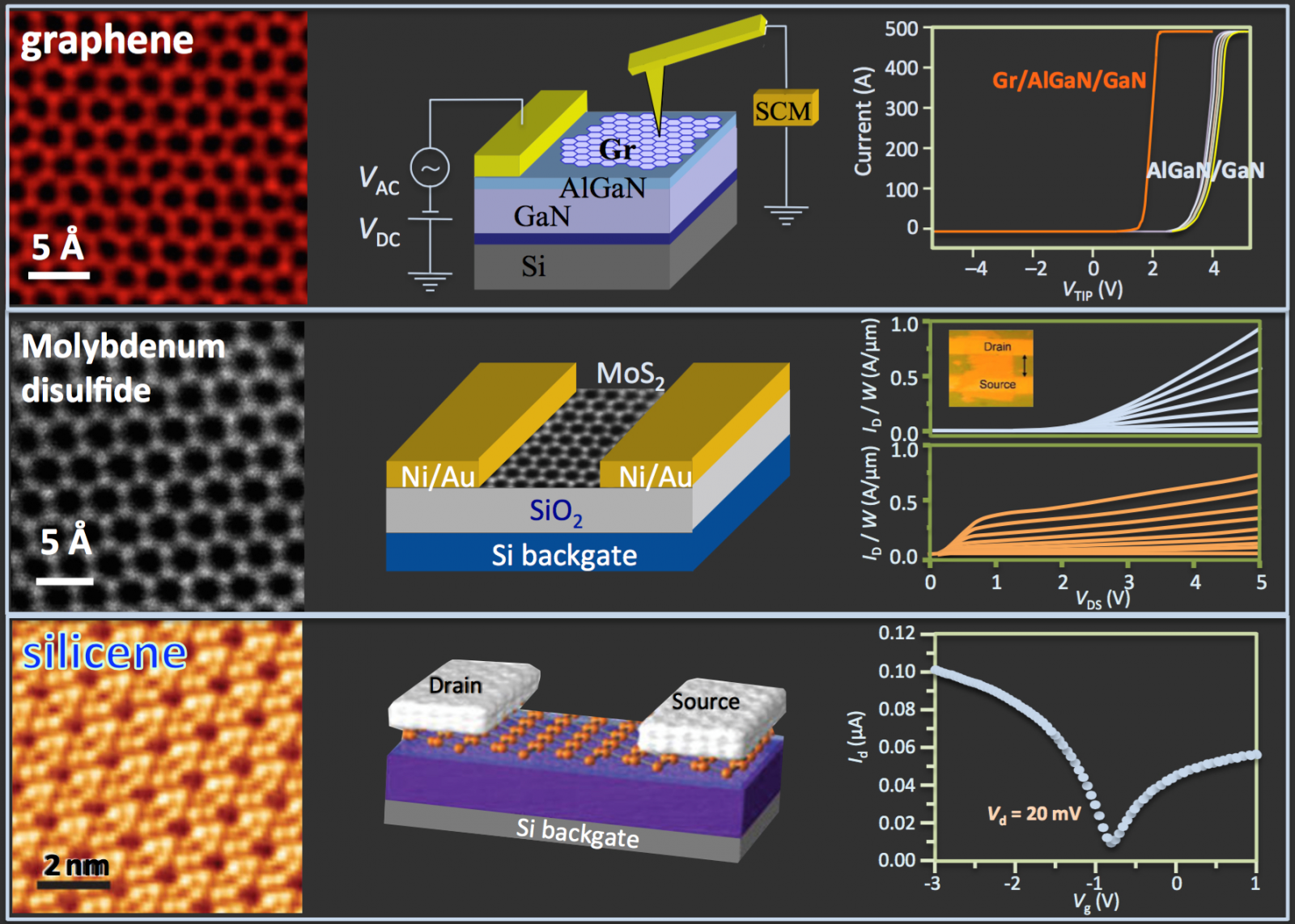
Exploring matter with increasing spatial resolution is not only the answer to our pure scientific curiosity, it is also a crucial challenge aimed to improve our capability to control physical properties of materials used for a variety of technological applications. In the field of microelectronics, for instance, one of the main motivation that has been driving our effort to improve performances of microscopy techniques is related to the consequences of a pure economic law, the one introduced by Gordon Moore, the co–founder of Intel, back to 1965. The Moore’s law states that the price per million of transistors or, similarly, the price per million of instructions processed per second, reduces by 35% per year, following a logarithmic trend. The effectiveness of this law strictly depends on our capability to progressively shrink the size of a single transistor we are able to fabricate in a silicon chip. This technological progress has been made possible, for a significant extent, thanks to our capability to explore matter with an increasing level of spatial resolution, by introducing emerging and more powerful microscopy techniques, moving from optical, to transmission electron microscopy (TEM) and, more recently, to spherical aberration–corrected scanning–transmission electron (STEM) microscopy. Such high spatial resolution techniques are extremely important to investigate matter at the atomic level and, from the technological point of view, in the field of microelectronics, to effectively face the ultimate limit of the silicon technology. Indeed, as the characteristic length of the elementary transistor will reduce to a distance below 10 nm, direct quantum mechanical tunneling of carriers, from the source to the drain of the device, may prevent any deterministic control of its electrical characteristics. This is believed to be the major bottleneck for the further scaling of this technology, and in many cases the solution to overcome these intrinsic obstacles is to introduce novel materials, device architectures, and complex heterostructures. The talk will address the importance of scanning transmission electron microscopy in characterizing materials of interest for the future trend in microelectronics, with applications ranging from phase–change materials, novel semiconductors, to two–dimensional materials.
